For the 4 g/LTE and the cloud era, electronic verification test industry - iST appropriate technology announced, according to the quality of the printed circuit board (PCB), with Acoustic Emission test (& Emission, AE).This method will help the cloud base stations/server PCB manufacturer, sheet in r&d stage, be determined to choose which kind of copper foil printed circuit board (CCL) materials, the most suitable for the process environment, to overcome the defects of welding plate hole crack.
Should be observed, solder hole crack phenomenon, is below the PCB solder produce cracks, it most commonly occurs in the cloud server, communication base stations on the use of high frequency high speed PCB;There are two main reasons, one for high-frequency high-speed material properties, the material sticking strength weak faults.Second, for the lead-free halogen-free requirement that material properties to rigid, assembly process, vulnerable to external mechanical stress, fracture in the form of welding plate hole defects.
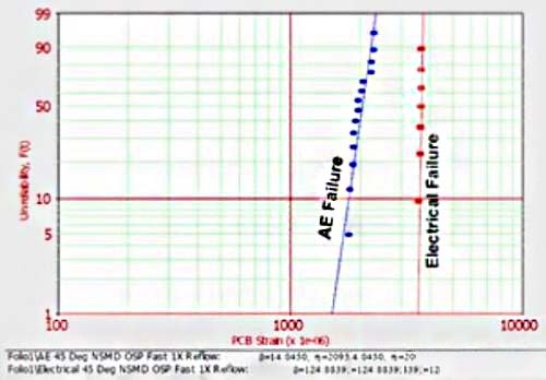
Welding plate hole crack defects, however, cannot be in the assembly process and outgoing inspection, detected by electrical test and appearance, because the general internal micro cracks of PCB material, won't produce an electrical failure, so that most producers cannot early detection of cracks in PCB materials.
"If the product into the market is used, although short-term use no problem, but this hole cracking phenomenon, like unexploded bombs, in the long run will significantly affect the operation of the product stability, produce the guest back issue, especially with high reliability requirements of the cloud base stations/server device."
To detect the PCB solder hole crack, and make up for the shortage of electrical test, appropriate, with international netcom company in recent years, the United States IPC (international Electronics industry join Association, Association Connecting Electronics Industries) to test and the development of acoustic emission (AE).IPC headquarters of the United States is at the end of 2013 will be released this method to the IPC 9709 standard, appropriate, the way and the formal import, this month to help the customer to confirm the quality of the product.
Acoustic emission testing technique, commonly used in earthquake monitoring or the building and the strength test of aviation materials;The appropriate transfer this method used to test on PCB.Use of plate bending test at the same time, by means of AE sensor detection plate under stress to produce micro crack is caused by sound waves, complete detection of the plate plane stress after the crack location, and detect its energy intensity.Thereby, detect high frequency printed circuit materials, welding plate hole crack resistance.
Caption: left failure analysis for red ink as a result, the right to cross section failure analysis results.Above samples through electrical testing, failure didn't happen, but through the AE can detect crack under above, solder.And through red ink and transverse failure analysis case, actually existing crack in the plate.
AE acoustic emission testing, will be able to assist in PCB suppliers, in the selection of copper foil printed circuit board (CCL) material stage, through the quantitative method, clarify the process in different environment, what kind of material is most suitable for its use, to overcome the defects of welding plate hole crack.


 Blog
Blog