The introduction
Acoustic emission technique is the combination of the optical fiber sensing technology and acoustic emission technology, is currently the trend of the development of acoustic emission technology. It will high sensitivity ae sensor installed on the surface of mechanical components to form a certain number of sensor array, real_time receiving and collection from the material defect of the acoustic emission signal, and then through the recognition of the acoustic emission signal, judgment and analysis to research on material damage defect testing and strength of component, such as damage, life is analyzed and studied.
At the scene of the actual component testing, sound source signal is usually between 100 ~ 800 kHz high_frequency weak signal, and the material damage detection, acoustic emission source location often require multiple sensors form the sensor array, and the acoustic emission signal data transmission system must reach more than 640 Mbps data transmission ability; And should have to deal with sudden or long time data receiving and storage capacity. This paper is to use CPLD to implement the acoustic emission signal acquisition, thus effectively solved the data real-time transmission and storage problem.
1 system design
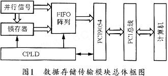
This scheme adopts the FIFO memory constitute external large capacity data buffer, DMA transmission way and the microcomputer using PCI bus for high_speed data transmission. The acoustic emission signal after AD conversion and drive circuit drive into the PCI interface card, and then some data latches, converts parallel signal to a serial parallel signals at the same time, through CPLD control logic circuit in the FIFO. When data arrives at a certain condition, the FIFO memory CPLD control logic will produce the interrupt signal to the bus controller PCI9054, which starts after DMA transfers data from the computer memory. DMA transfer is complete, channel interrupt PCI9054, and remove data from the memory by a computer in the hard disk. The overall diagram of the data transmission module is shown in figure 1.

2 FIFO data storage circuit design
FIFO is a ancestors first out of double buffer, to guarantee the normal work of the whole system, FIFO memory allows the system to the DMA operation, in order to improve data transmission speed. Otherwise, the data transmission will not reach requirement, and will greatly increase the burden of the CPU, or even complete data stored at the same time.
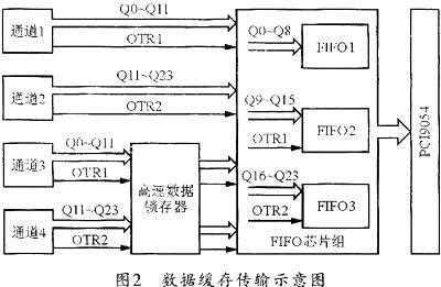
This design in data transmission system USES the six pieces of IDT72281 chip to cache the data, and is divided into two groups, one word wide extension by three pieces of FIFO, shown in figure 2 is the cache transmission schematic diagram. According to this design, the word width can be up to 27, 24 bits of data transmission and two OTR.

3 CPLD logic control
Due to the high speed signal processing in this system, therefore, to control the signal timing requirements are more strict. On the choice of control chip to choose as far as possible the time delay is small, the high speed chip. This design adopts the American Altera company MAX7000S series programmable logic device EPM7128SLC84 to 15, and USES the MAX + Plus Ⅱ to complete the system input, compile, validate, and programming, and then complete the vector test and simulation. The final data line can be downloaded to the chip to complete the configuration of the chip.
3.1 CPLD logic control circuit
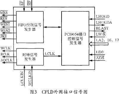
CPLD to sampling controller core, and strictly sequential control relationship is required for data transmission by the CPLD is responsible for processing. It in this system is mainly responsible for produce with PCI9054 handshake signals piece selected, data storage and read/write control signals. CPLD peripheral signal interface as shown in figure 3.

CPLD can be produced according to the requirements of the FIFO memory sequential control control signal, and the data in the first clock cycles were deposited in the FIFO and data latch 74 ls373, in the second clock cycles to latch the data stored in FIFO, so as to complete the parallel data to the serial data conversion. According to the relevant signal sent PCI9054 controller of storage at the same time interrupt request, and to read the data generated when PCI9054 corresponding control logic.
3.2 CPLD control logic
After the parallel data into the card, CPLD first deposit will be part of the data with the latch, and the other part of the data directly in the FIFO. But this must be the write clock signal WCLK binary frequency, in order to complete an AD conversion cycle twice FIFO write operations. When data arrives at half full FIFO, CPLD to PCI9054 interrupt application, and by PCI9054 the application into the computer. If the response of the system, please, in the interrupt response program read command, to read bytes and address signal, etc.
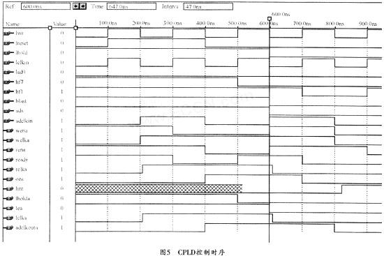
PCI9054 LOCAL bus control by LHOLD applications, while CPLD by LHOLDA response, so that the PCI9054 LOCAL control of the bus. PCI9054 will first PCI address mapping between narrow to a local address space, and then start a local bus of the DMA cycle. CPLD received read signal gating signal (LW/R), address (ADS) and address (LA16, LA17) after began to transmit data. When LA16 0, LA17 bits to 1, the system will lead to read can after three slices of FIFO (REN2) can make end, so that after three piece of Q0 ~ Q31 effective on a FIFO data line and at the same time also make PCI9054 READY signal (READY), effective data transmission. Before the last data transfer, BLAST signals effectively, after, CPLD will make FIFO read after one clock cycle can make (REN1 or REN2) is invalid, so as to complete a data transfer process.
3.3 control program design
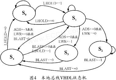
Read, write, and DMA PCI9054 single cycle of VHDL language sequential control state machine design as shown in figure 4. Diagram, S0 to idle state. When the local bus LHOLD request signal is set 1 to S1, otherwise stay S0. S1 for the bus to maintain state, the state should be local bus response signal LHOLDA 1. Such as ADS signal is 0 and LW/R is 1 was transferred to the S3, such as ADS signal is 1 and LW/R and BLAST to 0 to S4, this state indicates that the read operation for single cycle. S2 for DMA read state, in this condition should be READY signal and FIFO reading can make signal REN1 0. Such as BLAST is 1, indicates the DMA read has yet to be completed, should remain in S2, such as BLAST is 0, indicates the DMA read complete, can be transferred to S4. S3 writing status for the single cycle, this condition also want to buy the READY signal 0 "to write the data effectively, and when the BLAST of 0 to S4. S4 for the completion status, read and write operations is 0, when LHOLD means PCI9054 request local bus, no longer at this time should be transferred to S0, when the BLAST of 0 and LHOLD for 1, show that PCI9054 data read and write, reason should be transferred to S1 to continue operating.

The simulation results of the 3.4 control program logic
MAX + PLUS Ⅱ Aletra FPGA/CPLD series products of the company is the development of software tools, this design using the tools provided by the design environment and tools for development and debugging of CPLD control program. Its function sequence as shown in figure 5.

The design of CPLD with VHDL programming. The design operation code have been through the simulation, and applied in the actual debugging.
4 system driver design
This design use DriverWorks DriverWizard to create WDM framework program. Can add the program code according to the design demand, so as to complete the PCI device driver DMA transfer system, to perform a DMA operation, access I/O port and memory space and processor interrupt and access to the PCI. According to the requirements of the system, driver is the key to the following three aspects: hardware access, interrupt handling and DMA transfers.
KdmaAdapter class can be used to set up a DMA adapter, to indicate a DMA channel features and provide serialized access services; KDmaTransfer class is used to control the DMA transmission and start the DMA transfers, physical address and the number of bytes to transfer the DMA data buffer, after the DMA transfer, data will be used by common buffer copy to application data buffer; KCommon DmaBuffer used to implement the operation of the common buffer. For the DMA operation, this system also provides a special memory, namely common buffer. Should be clear, common buffer is a rare system resources, waste to use should be avoided.
5 conclusion
Data cache are given in this paper, the transmission module control circuit design, and USES the VHDL language and CPLD logic control task and writing and debugging of system driver. The experimental results show that the data transmission module of hardware, software, work is very reliable, stable, can achieve 640 Mbps (more than 80 MByte/s) real-time data storage and transmission, can fully meet the requirements of acoustic emission signal acquisition.
References (abbreviated)
